Yesterday I played around with cardboard to have a better (physical) sense of the first housing version. In short, this housing will be the simplest I can build to fit the Mainboard and an Atreus keyboard. Nothing fancy, not even an internal routing of the USB cable. In the end I want to build momentum and, considering the blocks of time I can allocate to this project, I figured it would be best to use (very) small increments.
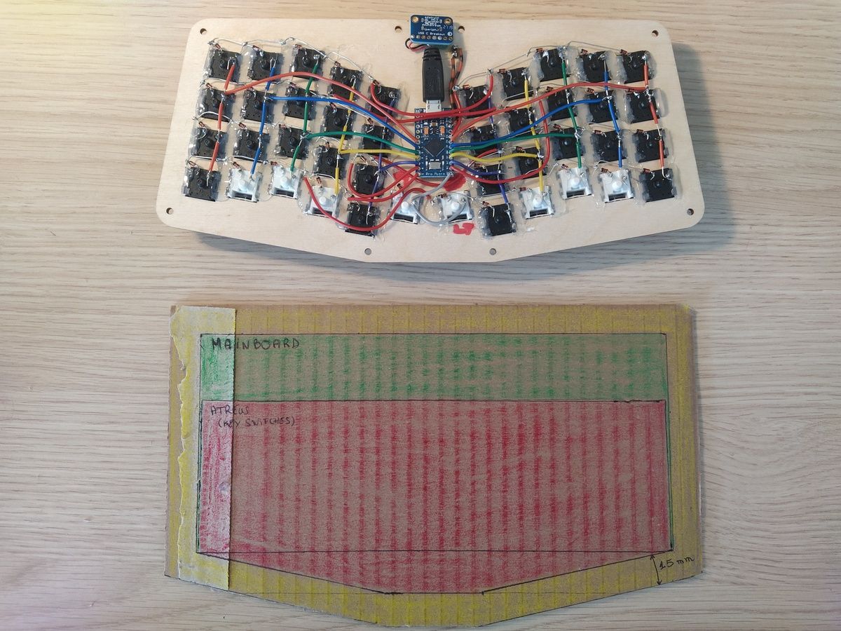
Laying out the Mainboard and the Atreus side-to-side on a piece of cardboard (cut to be as wide as the Atreus case is) really shows how similarly sized the two elements are. Let's cut another template for the Atreus' PCB layer (the layer, either PCB or plywood, that holds the key switches) and fit them together.

I came up with two possible designs to optimally fit the Mainboard (roughly 232×104mm) and the PCB layer of the Atreus (roughly 226×90mm in its rectangular form, otherwise the shorter side is down to 72mm). The first one (bottom in the following picture) is simply placing the keyboard on top of the mainboard, aligning them at the bottom. This really is the minimum form factor I can come up with right now (that is, without using a sturdier housing material to make the walls thinner). The second option is to keep the Atreus split angles and letting it slip past the Mainboard bottom side.
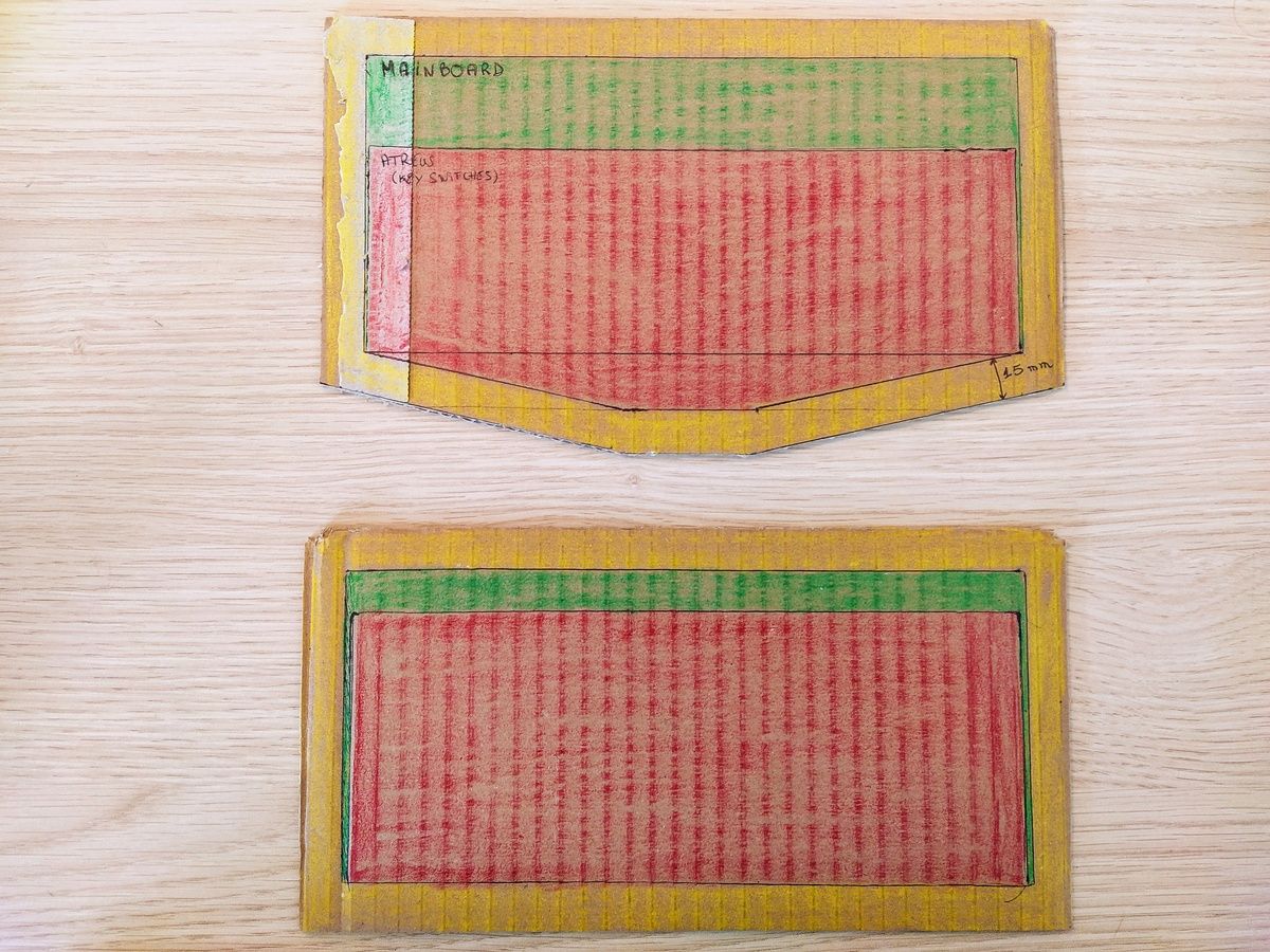
Obviously the second is design is preferred because otherwise there would be a lot of "blank" housing on the left and right most side of the keyboard, denying the advantage the split angles the Atreus offers. The first design would be relevant for a plain (ortholinear) matrix-style keyboard. But I am fine making the housing slightly larger to keep the split angles.
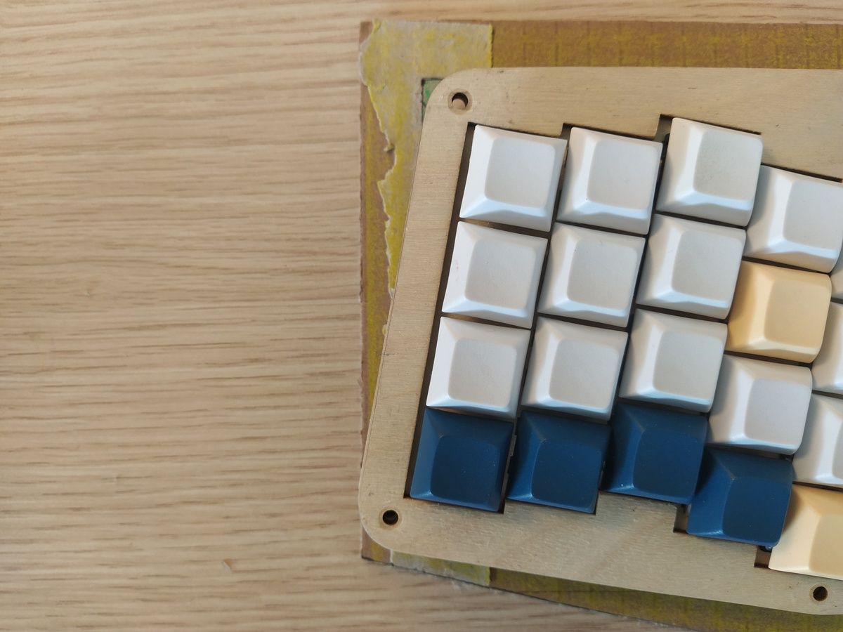
To illustrate the size taken by the Atreus PCB layer, see the following picture. It would be the shape that encloses all key switches.
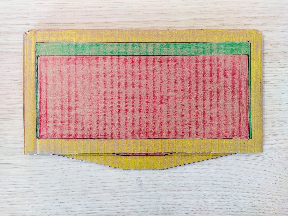
As can be seen on the following two pictures, the housing design is very close to the original Atreus footprint; I actually used the width of the Atreus as a guide here. The major difference is that the thickness will be approximately doubled.